(Hong Kong)

Product Summary
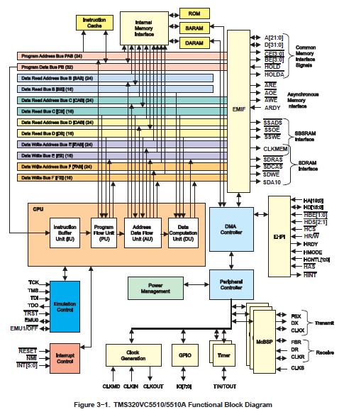
The TMS320VC5510AZGW2 is a fixed-point digital signal processor (DSPs). The TMS320VC5510AZGW2 is based on the TMS320C55x DSP generation CPU processor core. The TMS320VC5510AZGW2 architecture achieves high performance and low power through increased parallelism and total focus on reduction in power dissipation. The CPU supports an internal bus structure composed of one program bus, three data read buses, two data write buses, and additional buses dedicated to peripheral and DMA activity. These buses provide the ability to perform up to three data reads and two data writes in a single cycle. In parallel, the DMA controller can perform up to two data transfers per cycle independent of the CPU activity.
Parametrics
TMS320VC5510AZGW2 absolute maximum ratings: (1)Supply voltage I/O range, DVDD: -0.3 V to 4.0 V; (2)Supply voltage core range, CVDD: -0.3 V to 2.0 V; (3)Input voltage range, VI: -0.3 V to 4.5 V; (4)Output voltage range, VO: -0.3 V to 4.5 V; (5)Operating case temperature range, TC: (Commercial): 0℃ to 85℃; (6)(Extended): -40℃ to 85℃; (7)Storage temperature range, Tstg: -55℃ to 150℃.
Features
TMS320VC5510AZGW2 features: (1)High-Performance, Low-Power, Fixed-Point TMS320C55x Digital Signal Processor (DSP): 6.25-/5-ns Instruction Cycle Time; 160-/200-MHz Clock Rate; One/Two Instructions Executed per Cycle; Dual Multipliers (Up to 400 Million Multiply-Accumulates Per Second (MMACS)); Two Arithmetic/Logic Units; One Internal Program Bus; Three Internal Data/Operand Read Buses; Two Internal Data/Operand Write Buses; (2)Instruction Cache (24K Bytes); (3)160K x 16-Bit On-Chip RAM Composed of: Eight Blocks of 4K × 16-Bit Dual-Access RAM (DARAM) (64K Bytes); 32 Blocks of 4K × 16-Bit Single-Access RAM (SARAM) (256K Bytes); (4)16K × 16-Bit On-Chip ROM (32K Bytes); (5)8M × 16-Bit Maximum Addressable External Memory Space; (6)32-Bit External Memory Interface (EMIF) With Glueless Interface to: Asynchronous Static RAM (SRAM); Asynchronous EPROM; Synchronous DRAM (SDRAM); Synchronous Burst SRAM (SBSRAM); (7)Programmable Low-Power Control of Six Device Functional Domains; (8)On-Chip Peripherals, Two 20-Bit Timers; Six-Channel Direct Memory Access (DMA) Controller; Three Multichannel Buffered Serial Ports (McBSPs); 16-Bit Parallel Enhanced Host-Port; Interface (EHPI); Programmable Digital Phase-Locked; Loop (DPLL) Clock Generator; Eight General-Purpose I/O (GPIO) Pins and Dedicated General-Purpose Output (XF); (9)On-Chip Scan-Based Emulation Logic; (10)IEEE Std 1149.1. (JTAG) Boundary Scan Logic; (11)240-Terminal MicroStar BGA. (Ball Grid Array) (GGW Suffix); (12)240-Terminal MicroStar BGA. (Ball Grid Array) (ZGW Suffix) [Lead-Free]; (13)3.3-V I/O Supply Voltage; (14)1.6-V Core Supply Voltage.
Diagrams
| Image | Part No | Mfg | Description |  |
Pricing (USD) |
Quantity | ||||||||||||
|---|---|---|---|---|---|---|---|---|---|---|---|---|---|---|---|---|---|---|
 |
 TMS320VC5510AZGW2 |
Texas Instruments |
Digital Signal Processors & Controllers (DSP, DSC) Fixed-Point DSP |
Data Sheet |
|
|
||||||||||||
| Image | Part No | Mfg | Description | |
Pricing (USD) |
Quantity | ||||||||||||
 |
TMS3112 |
Other |
|
Data Sheet |
Negotiable |
|
||||||||||||
|
TMS3121 |
Other |
|
Data Sheet |
Negotiable |
|
||||||||||||
|
TMS320 |
Other |
|
Data Sheet |
Negotiable |
|
||||||||||||
|
TMS32010 |
Other |
|
Data Sheet |
Negotiable |
|
||||||||||||
|
TMS320AV7110 |
Other |
|
Data Sheet |
Negotiable |
|
||||||||||||
|
TMS320BC51PQ100 |
Texas Instruments |
Digital Signal Processors & Controllers (DSP, DSC) TMS320C51PQ - 132QFP - 100MHZ/BOOT CODE |
Data Sheet |
Negotiable |
|
||||||||||||